Incorporated in 1986, Lintek is an Australian manufacturer of printed circuit boards. Located close to Canberra, the nation’s capital, the company has access to both international and domestic freighting facilities.
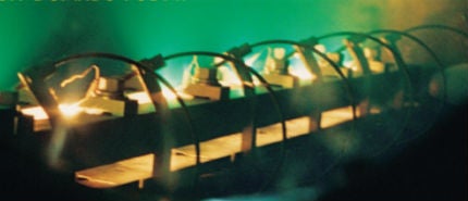
Lintek is one of the most innovative printed circuit board (PCB) companies in the world, with its patented high-vacuum copper deposition process to establish the initial copper seed layer. This enables the manufacture of a large variety of printed circuit boards, ranging from 1.8m-long antennas to sub-miniature transmitters, using a variety of different substrates.
PCBs on standard FR4, PTFE Teflon and ceramic-based materials
Lintek manufacture PCBs on a variety of materials from standard FR4 to exotic dielectric PTFE Teflon and ceramic-based materials.
Although we typically supply PCBs for RF, microwave, high frequency, phased array radar and EW applications, Lintek manufactures a range of PCBs from single and double sided to mixed dielectric multilayers, metal-backed PTFE with blind vias, for prototype and production volumes.
PCB testing and verification
Lintek has gained the following accreditations:
- Quality System AS/NZS ISO 9001:2008 compliant
- Underwriters Laboratories (UL) Approval File Number EI24884
- Certified IPC-A-600 trainer and all inspectors certified IPC-A-600 specialists
Lintek manufactures PCBs, meeting the demands for commercial, government organisations and principle defence contractors, both locally and internationally. We supply directly and indirectly into long-life programmes.
Our products are electrically tested and inspected to the IPC-A-600 acceptability standards. Compliance certificates are available on request.
Highly accurate PCBs
Lintek’s continued success in this internationally competitive industrial sector rests on our worldwide patented vacuum copper deposition process, designed and built by Lintek, which we have been recognised for and presented with National Excellence Awards. The Lintek process has many advantages over conventionally manufactured printed circuit boards.
These are as follows:
- The process does not require chemicals to grow the initial conductive copper seed layer, which greatly reduces the chemical usage and waste generated in the manufacturing process
- After electroplating the circuits to the required thickness, only 1-2 micron copper seed layer has to be removed, compared with the conventional 18 micron base copper layer, eliminating the need to use an etch resist, such as tin
- Significantly less etching is required to remove the 1-2 micron seed layer, eliminating undercut, ensuring the repeatability of very fine track and spaces, accurate copper features and filters, near perfect side wall resolution, superb impedance control and high bond strength to exotic substrates
- The plated through holes are stronger and more reliable as a result of the same amount of copper being deposited in the plated through hole as on the surface, which is particularly important on PTFE materials, which have a large thermal expansion in the Z direction
- The elimination of reducing the copper thickness to achieve accurate copper features for impedance control
- The sodium etch process is elimination with PTFE materials
Although our technology and manufacturing process produces features ideal for high-frequency RF and microwave applications, the process advantages and unrivalled accuracy are maintained when processing standard materials, such as FR4.
Environmentally friendly PCBs
In addition to having many advantages over conventionally manufactured PCB features, Lintek’s vacuum copper deposition process eliminates many of the chemicals and processes required using the conventional manufacturing process.
The process significantly eliminates many environmentally dangerous chemicals required for the manufacturing process and disposal. These include palladium chloride, formaldehyde, complex coppers, reducing agents, stannous chlorides, sodium etch, tin plating, tin stripping, etc. This ensures a more efficient process and a reduction of waste so that our pricing remains competitive and our environment cleaner.


